Files and steps for completion of the PCB Milling Assignment
Please download the 555timerCES folder to begin this step of the assignemnt.
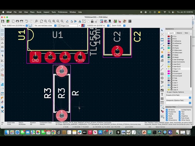
To complete this step, you must arrange and route connections between the components of the 555 timer LED flasher circuit inside KiCAD's PCB editor. There are three tutorial videos for this section. The first move through the whole process in detail and also gives context for the layout process in reference to the milling and assembly portion of this assignment. The second video is much shorter and runs through the process with little explanation. It is meant to be watched after the first video and to be a reference as you're doing the assignment. The third is an optional tutorial on more flexible custom board outlines imported from the internet or made yourself in programs like Inkscape.
Detailed tutorial:
NOTE: Please remember when you're doing your board layout to have your design fit well within the bounds of 152mm x 106mm (your design will most likely be much smaller than this, but just in case you're feeling experimental), which is the maximum size of the copper board you have to work with.
Reference tutorial:
Additional tutorial for custom board outlines (SEE CORRECTION AFTER THIS VIDEO):
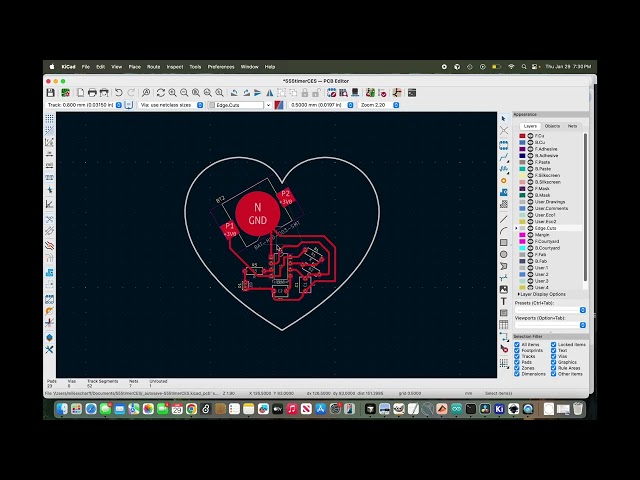
CORRECTION TO PREVIOUS VIDEO: I neglected to say that when you're importing you custom board outline .svg file, you must select the layer as "Edge.cuts" in the same pop-up window as you set the scaling. I left the layer as "User.drawings". Please see the image below on where to select the layer.

In this step, we will convert our gerber and drill files generated by KiCAD from out PCB layout into .svg files suitable for milling our PCB. We will use a shell script provided in this github called pcb_to_easel.sh to do this. I've provided a guide in this github as well, PCB_TO_EASEL_USE_GUIDE.md, that details the dependencies and what you need to alter in the shell script. Below is a video detailing the process of using the script.
In this step, we use the .svg files we generated in Step 2 to mill our PCB on the Carvey CNC. It's important to note that there is no perfect way to do this process. Small physical initial conditions can change the result of your mill, and it's important to be able to adjust. In the tutorial video below, some of the results of my milling are unexpected, and I show how I respond and adapt to these results. The milling of your traces is most likely going to be the most likely going to take a few tries a different depths, as I show in the video. Also, I'm going to recommend that for your drill holes and your board outline that you utilize the "add depth" feature in Easel and add an additional 0.2mm up front. I show this in the video, though I end up adding the depth after an initial cut, and forget to do so when doing the drill holes. YOU MUST WATCH THIS TUTORIAL VIDEO AND UNDERSTAND THE PROCESS BEFORE YOU ATTEND YOUR CNC SESSION IN THE LAB.
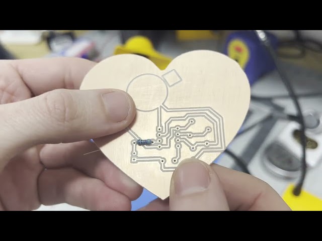
In the tutorial for this step, we choose component values to control our LED flashing frequency, and talk about techniques for soldering your components to your milled circuit board. Please note that due to voltage limitations of the CR2032 coin cell battery, we can only use red and yellow LEDs. Also we are using ceramic capacitors, NOT electrolytic. If you're confused what I mean, please refer to the two boxes in which I retrieve capacitors from in the video.