
The HP Integral PC was a portable 68000 UNIX based computer introduced in 1984. The computer included a floppy drive as mass storage and a printer was built in. The screen was a electroluminicent screen. The computer has a HPIB connector to attach to external devices. External disks can be attached through HPIB.
The computer has a two expansion slot where various peripherals can be installed. For example serial boards or memory expansion boards. It was also possible to install ROM boards. The software engineering ROM has 2Mbyte of ROM expansion and when installed appear as 8 disk devices in the Unix system.
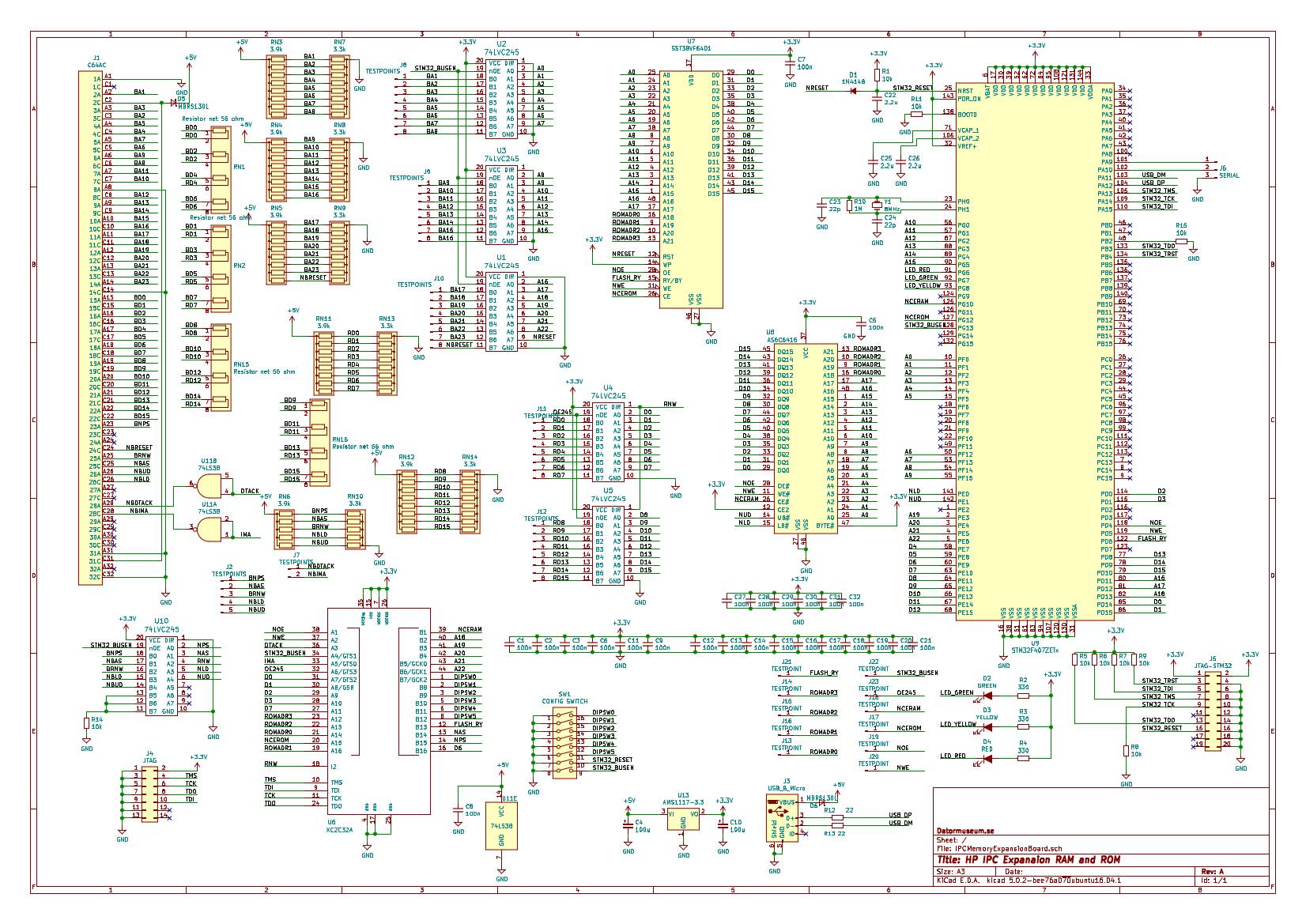
The project aims at creating a 7M RAM and 8M ROM memory expansion to the HP Integral computer. RAM is implemented using a single SRAM chip and ROM is implemented using a single NOR FLASH ROM chip. DIP-switches are used to map the ROM into the various ROM areas of the Integral.
All signals are level shifted from 5V TTL to 3.3V LVTTL using six 74LVC245 which has 5V tolerant inputs. The two open-collector signals, NBDTACK and NBIMA is handled by 1 74LS38 chip.
A Xilinx XC2C32A CPLD is used for all address decoding and ROM remapping. The VHDL is provided here.
The board is using a piano-type dipswitch for easy access from the side. When the switch is in the up position in corresponds to the off condition or digital 1 signal. When the switch is in the down position this corresponds to a on condition or 0 signal. X means that the position of the switch is irrelevant.
DIPSW0 to DIPSW5 is used for controlling the ROM mapping in the address space.
DIPSW7 is used for enabling and disabling the busdrivers and DIPSW6 is connected to RESET of the processor. Thus the processor portion can be completely disabled when both these switches are pushed down (on). They should be in the UP (off) position so that the processor runs and can access the memory when trying to upload to the flash memory onboard. When used in the Integral PC they should be in the DOWN (on) position to stop the processor and disable processor access to the memory.
The mapping of the FLASH ROM memory is controlled by six dipswitches as follows:
| Integral address range | DIPSW0 | DIPSW1 | DIPSW2 | DIPSW3 | DIPSW4 | DIPSW5 | Flash memory range | Used for |
|---|---|---|---|---|---|---|---|---|
| 000000 - 07FFFF | Down(0) | Down(0) | X | X | X | X | 000000-07FFFF | SYS V ROM |
| 000000 - 07FFFF | Down(0) | Up(1) | X | X | X | X | 080000-0FFFFF | DiagA ROM |
| 000000 - 07FFFF | Up(1) | Down(0) | X | X | X | X | 100000-17FFFF | DiagB ROM |
| 000000 - 07FFFF | Up(1) | Up(1) | X | X | X | X | NONE | Internal ROM used |
| 080000 - 0FFFFF | X | X | Down(0) | X | X | X | NONE | NONE |
| 080000 - 0FFFFF | X | X | Up(1) | X | X | X | 180000-1FFFFF | BASIC ROM |
| 100000 - 1FFFFF | X | X | X | X | X | Down(0) | NONE | |
| 100000 - 1FFFFF | X | X | X | X | X | Up(1) | 600000-6FFFFF | AUX ROM 3 |
| 200000 - 3FFFFF | X | X | X | Down(0) | Down(0) | X | 200000-3FFFFF | SE ROM |
| 200000 - 3FFFFF | X | X | X | Down(0) | Up(1) | X | 400000-5FFFFF | AUX ROM 1 |
| 200000 - 3FFFFF | X | X | X | Up(1) | X | X | NONE | NONE |
| 300000 - 4FFFFF | X | X | X | X | X | Down(0) | NONE | NONE |
| 300000 - 4FFFFF | X | X | X | X | X | Up(1) | 700000-7FFFFF | AUX ROM 2 |
There is a STM32F407ZET SoC makes the board look like a USB stick when the USB port is connected to a host computer.
The ROM is implemented in one single 8 Mbyte SST38VF6401 chip.
Normally Integral memory is implemented using memory board sized up to 1 MByte. Each memory board responds to a read port which provide an ID for the board and a writable base address register. The Integral will use these to identfiy each memory board and configure its starting address. However the memory sizing of HP-UX system is completely independent of the memory configuration descibed preiously meaning that these configuaration is not necessary to get the Integral to detect the full memory. This has been verified using the MAME emulation of the Integral.
All this obviously that it would be very much easier to implement a RAM expansion board since it only requires that it would match the RAM address range 800000-EFFFFF.
The RAM is implemented in one single AS6C6416 4M x 16 SRAM memory chip.
Obviously when testing the board for the first time it didn't work at all. Of course I tested many different ways to get it working. But in the end I think that one main problem was the use of UDS/LDS instead of AS strobe. On the standard 68000 that would probably have worked just fine. But on the HP Integral he AS strobe is not at all the AS strobe from the processor. It has gone through plenty of logic until the AS signal found in the expasion connector is generated. Thus the use of the AS signal is a must. Gating with that signal made the RAM expansio work fine.
Since the 74LVC245 inputs are CMOS there wil be no current flowing towards the expansion board. When I attached a bus extender board to be able to measure on the board the added buslength seemed to cause trouble. Adding bus terminating resistors at the 74LVC245 inputs seemed to fix the issue. To better adapt the 74LVC245 driver to the bus impedance a low ohm resistor was inserted in the bus line path for the data bus.
All these changes resulted in a second spin of the board.

Spin 1 became quite messy when trying to fix all small problems so I decided on a spin 2. I also added test points to make it easier to measure on the board, a major issue on the first spin was that it was so hard to take measurements. After spin 2 came back from the JLCPCB I found that it was virtually impossible to get hold of the STM32 chip and the CPLD, so the project got dormant until sping 2023 when I eventually was able to order chips.
There were some small changes made to the CPLD VHDL code for spin 2 which to this date has not yet been tested (2023-07-24). I hope to be able to test the board soon.
Spin 2 has now been tested and appears to work correctly. Follow instructions further down to install the board.
There are two firmwares. One Arduino style .ino-sketch which I used for testing and the a STM32Cube applicaton that is the production code. I used STM32 because it was so simple to wrap up the USB mass storage stuff. The code essentially enables the FSMC controller of the chip and enables the USB mass storage code, then it responds to read and writes to the memory. While the USB-cable is connected the green LED will blink. The yellow LED will blink when a read is performed and the red will blink when a write is performed.
There are three steps that need to be taken to install the all needed software/firmware to get the board running.
- Program the CPLD
- Install the STM32 firmware
- Upload integral software to the board
For all these steps the USB connector of the board need to be connected to a USB outlet to the computer. This will thus supply the board with power and in the third step also make the board able to communicate with the host.
The CPLD code is written in VHDL and I have used the Xilinx ISE version 14.7. In order to just install the existing JEDEC file provided in the repo it is only necessary to use the Impact tool in the Xilinx ISE suite. Download, start Impact, attach the Xilinx download cable and make sure that the device is detected. Then select the main.jed file and program the device.
You need both the STM32CubeIDE and STM32CubeProgrammer which has to be downloaded from the ST webpage. Use defaults when installing the software.
When installation is ready start STM32CubeIDE and select the "Open Projects from file System" option in the menu. Select the folder " Software/STM32CubeIDE/workspace_1.7.0 /HP IPC Memory Expansion/" in this repo. In the project menu, select the Build Configurations. This will open a submenu which where you can do "Set Active" Select "Release"
Now do "Build All" from the project menu and the full software will be built.
Now start the STM32CubeProgrammer software nd make sure the STM32 download canle is attached to the board and that power is supplied to the board using the USB cable. In this step DIPSW 6 and DIPSW 7 has to be in the up posistion.
Select the "HP IPC Memory Expansion.elf" binary in the Release folder and do a "Erase and program" operation.
The idea is to use the Linux dd command to transfer the image-file generated by the build.sh shellscript in ROMS folder. When doing so the red and green LEDs should blink. It should also be possible to read back the content stored using dd and compare with the actual file. It is important to write the image to the topmost 8M of the USB device created when the board is connected over USB. The top 8M is mapped to the flash memory while the lower 8M is mapped to the SRAM.
Thus this command is needed to write the flash:
sudo dd if=flash_image.bin of=/dev/sd<x> bs=1k seek=8192
where /dev/sd<x> is the device that is allocated for the mass storage device that the board is acting as. Check using dmesg what device is created when it is plugged into the USB-port.
After spin 1 was completed I was not able to get components for spin 2 although the board had been fabricated. All this due to the post-covid semiconductor crunch. In July 2023 I got contacted by Carl who had been asked to help out to do the installation of the firmware. As we sorted out how topoerform the steps (which I had more or less forgotten since I initially designed it) he created a nice document which describes the steps do be done. I link it below:
Install instructions by Carl Claunch
This is a BOM for the spin 2 board:
| Component designator | Description | Mouser order number | Misc. |
|---|---|---|---|
| R1,R5,R6,R7,R8,R9,R11,R14,R15 | 10kOhm SMD 0805 | - | |
| R2,R3,R4 | 330 Ohm SMD 0805 | - | |
| R10 | 1MOhm SMD 0805 | - | |
| R12,R13 | 22 Ohm SMD 0805 | - | |
| RN1,RN2,RN15,RN16 | network 4 x bussed 56 Ohm THT | 652-4608X-2LF-56 | |
| RN3,RN4,RN5,RN6,RN11,RN12 | network 8 x star 3.9 KOhm THT | 652-4609X-1LF-3.9K | |
| RN10 | network 5 x star 3.3 KOhm THT | 652-4606X-1LF-3.3K | |
| RN7,RN8,RN9,RN10,RN13,RN14 | network 8 x star 3.3 KOhm THT | 652-4609X-1LF-3.3K | |
| RN6 | network 5 x star 3.9 KOhm | 652-4606X-1LF-3.9K | |
| C1,C2,C3,C5,C6,C7,C8 | 100 nF Ceramic THT, RM5 | - | |
| C4,C10 | 100 uF Electrolytic THT, RM 2.5 | - | |
| C9,C11,C12,C13,C14,C15,C16,C17,C18, C19,C20,C21,C27,C28,C29,C30,C31,C32 |
100 nF SMD 0805 | - | |
| C22,C25,C26 | 2.2 uF SMD, 0805 | - | C25 is on the underside just below the processor chip, close to C29. The silkscreen is a bit bad |
| C23,C24 | 22 pF SMD, 0805 | - | |
| D1 | IN4148 SMD | 750-1N4148W-HF | Located on the top side close to the processor |
| D2 | LED green 3mm THT | 859-LTL-4231N | |
| D3 | LED yellow 3mm THT | 859-LTL-4251N | |
| D4 | LED red 3mm THT | 859-LTL-4221N | |
| D5,D6 | MBRS130L SMD, 2010 | 78-VS-MBRS130L-M35BT | |
| SW1 | 8 DIP switch - piano style THT | 774-1958MS | |
| U1,U2,U3,U4,U5,U10 | 74LVC245 THT | 595-SN74LVC245ANE4 | |
| U6 | XC2C32A SMD | 217-XC2C32A-6VQG44I | |
| U7 | SST38VF6401 SMD | 804-38VF64019CEKE | |
| U8 | AS6C6416 SMD | 913-AS6C6416-55TIN | |
| U9 | STM32F407ZET SMD | 511-STM32F407ZET7 | |
| U11 | 74LS38 THT | - | |
| U13 | AMS1117-3.3 SMD | 621-AZ1117CD-3.3TRG1 | Mounted on the bottom side |
| Y1 | Crystal 8 MHz | 815-ABL-8-B2 | |
| J1 | C64AC, 2 x 32 pin, 90 deg angle THT | 617-09732647801 | |
| J2,J7,J13,J14,J15,J16,J17,J18, J19,J20,J21,J22,J23 |
Test points | - | Normally not needed |
| J3 | Mini USB | 710-65100516121 | |
| J4 | 2 x 7 pin header, 90 deg angle, RM 2.54 | - | JTAG for Xilinx CPLD |
| J5 | 2 x 10 pin header, 90 deg angle, RM 2.54 | 710-61202021721 | JTAG for STM32 |
| J6 | 3 pin header, 90 deg angle, RM 2.54 | 538-22-28-8031 | Serial output |
HP Museum page on the Integral PC
Peter Johnsons page on the Integral PC