Bi-Phase Encoder With Configurable Bitrate Based on CLB and DMA Using the PIC18F56Q35 Microcontroller With MCC Melody
The repository contains the Bi-Phase Encoder, an MPLAB® X project which uses Core Independent Peripherals (CIPs) by following the interaction between the Custom Logic Block (CLB), Direct Memory Access Controller (DMA) and Timer0 (TMR0) to achieve a CPU-less data processing architecture. The Universal Asynchronous Receiver-Transmitter (UART) is used for debugging and run-time verification via serial console.
The CLB peripheral is a collection of logic elements that can be programmed to perform a wide variety of digital logic functions. The logic function may be completely combinatorial, sequential, or a combination of the two, enabling users to incorporate hardware-based custom logic into their applications.
The Bi-Phase Mark Code (BMC) combines both data and clock into a single signal. One clock cycle is a BMC bit period. A transition always occurs at the beginning of each bit period. A logic ‘1’ is represented by a transition (rising or falling edge) in the middle of the bit period and a logic ‘0’ is represented by no transition in the middle of the period. A BMC encoder accepts a data signal and a clock signal as inputs and produces a single BMC-encoded output. A BMC decoder accepts a BMC-encoded signal as input and produces two outputs: data and clock. BMC is used in USB 3.1 Power Delivery Specification CC signaling, AES3 digital audio or S/PDIF audio standards; an example of this type can be seen in the figure below.

More details and code examples on the PIC18F56Q35 can be found at the following links:
- PIC18F56Q35 Product Page
- PIC18F56Q35 Code Examples on Discover
- PIC18F56Q35 Code Examples on GitHub
- Bi-Phase Decoder with Configurable Bitrate Based on CLB Using the PIC16F13276 Microcontroller with MCC Melody
- Bi-Phase Encoder and Decoder - Use Cases for CIPs Using the AVR128DA48 Microcontroller with MCC Melody
- MPLAB® X IDE v6.30 or newer or MPLAB® Tools for VS Code®
- MPLAB® XC8 v3.10 or newer
- PIC18F-Q_DFP v1.30.487 or newer
- The PIC18F56Q35 Curiosity Nano Development board is used as a test platform:


To program the Curiosity Nano board with this MPLAB X project, follow the steps provided in the How to Program the Curiosity Nano Board chapter.
This project is an implementation of a Bi-Phase encoder using CIPs by following the interaction between CLB, DMA and TMR0 to achieve a CPU-less operation. The raw data is streamed via DMA directly into the CLB, where it is encoded using a hardware-defined digital logic circuit. The timing of the encoding process is provided by TMR0, acting as the bit period clock, while the CPU is not involved in the data path. The encoded signal is then generated on a single output line. The UART peripheral is used for debugging purposes, allowing visualization of the transmitted data in the serial console. The CLB circuit is captured in the figure below:

The design includes a Parallel-In Serial-Out (PISO) shift register used to serialize input data loaded via the 8-bit long CLB Software Input Low (CLBINL) register, that can be used as destination for the DMA controller. The logic is driven by the TMR0 overflow signal acting as the bit clock.

The serialized data is further processed by the NRZ-to-BMC encoder block, which generates the final encoded output. Control signals, such as Encoder Enable, manage the data flow, while status signals (ACTIVE, RDY) indicate transfer activity. The entire data path is hardware-driven, with data supplied via DMA and no CPU intervention required.

The raw data is driven by the DMA controller, which transfers data directly from various memory sources such as Flash, EEPROM, Special Function Registers (SFR) or General Purpose Registers (GPR). This data is then used as input for the CLB-based PISO block, which generates a serialized Non-Return-to-Zero (NRZ) data signal synchronized with the clock provided by TMR0. These signals are further processed by the logic implemented inside the CLB peripheral, which outputs the Bi-Phase encoded signal.
After initializing all peripherals, a Start byte is used for synchronization purposes. The data is transferred by the DMA controller from a predefined memory source and streamed into the CLB input path. The DMA operates autonomously, feeding data byte by byte into the hardware logic without CPU intervention, following a predefined transfer sequence. A Start byte and a Stop byte can be used to delimit each message within the data stream.
The DMA transfer is triggered by the CLB_IRQ0 signal, ensuring synchronization between the CLB logic and the incoming data stream. This trigger is asserted either by the RDY signal generated by the PISO module, indicating that new data can be loaded, or by a software-controlled mechanism. The trigger occurs when a logic ‘1’ is written to bit 0 of the CLBINH register, provided that the write operation is validated by the Write Pulse status from the CLBINHWR input option of the CLB.
The CLBOUTL0 output is used as the final Bi-Phase encoded signal. The CLBOUTL1, CLBOUTL2 and CLBOUTL3 outputs are used for real-time debugging by routing internal PISO signals to external pins via the Peripheral Pin Select (PPS) module, allowing direct observation of the data path.
In this implementation, the BMC bit rate is controlled by adjusting the TMR0 period, which defines the duration of each bit transfer. Similar to configurable peripheral-based approaches, multiple typical frequencies can be selected, such as 31.25 kHz, 62.5 kHz, 125 kHz, 250 kHz, 500 kHz, 1 MHz.
Note: The timer frequency must be configured at twice the desired BMC frequency, as each bit period requires two timing intervals for correct encoding in the CLB design.
The following peripheral and clock configurations are set up using the MPLAB Code Configurator (MCC) Melody for the PIC18F56Q35:
-
Configuration Bits:
- CPU Halt bit: CPU operates normally after loading the Configurable Logic Block (CLB) / Special Function Register (SFR) image
- CLB Configuration on Start-Up: The CLB will not be automatically configured during device configuration
- WDT operating mode: WDT Disabled; SEN is ignored

-
Clock Control:
- Clock Source: HFINTOSC
- HF Internal Clock: 64_MHz
- Clock Divider: 1

-
CLB Synthesizer Library:
- Clock Divider: 8
- Clock Selection: HFINTOSC
- CLB Configuration Options: CLB configured after reset
- Enable CLB: Enabled

-
CRC:
- Auto-configured by CLB
-
TMR0:
- Timer Enable: Enabled
- Timer Mode: 8-bit
- Clock Source: HFINTOSC
- Prescaler: 1:8
- Requested Period: 500 ns

-
UART2:
- Requested Baud Rate: 115200
- Data Size: 8
- Redirect STDIO to UART: Enabled
- Enable Receive: Disabled
- Enable Transmit: Enabled
- Enable UART: Enabled

-
DMA1:
- DMA Enable: Enabled
- Start Trigger: CLB0
- Abort Trigger: DMA1SCNT
- Abort Trigger Enable: Enabled
- Source Region: Program Flash
- Source Address: 0
- Source Mode: incremented
- Source Message Size: 1
- Destination Region: SFR
- Destination Module: CLB1
- Destination SFR: CLBSWINL
- Destination Mode: unchanged
- Destination Message Size: 1


-
Pin Grid View and Pins:
- CLBOUTL0 - RD4 (BMC signal)
- CLBOUTL1 - RD5 (PISO RDY)
- CLBOUTL2 - RD6 (PISO DOUT)
- CLBOUTL3 - RD7 (PISO ACTIVE)
- UART2 TX - RB4
- LED0 - RC2


In this demo, a predefined message stored in Flash memory, PIC18F-Q35 CLB & DMA ENCODER, is transferred by the DMA controller directly to the CLB-based encoder. The message is delimited by a Start byte and a Stop byte, then serialized by the PISO block and converted into a Bi-Phase signal. The output of the encoder can be visualized using a logic analyzer.

To use the embedded decoder from the Logic software, the next analyzers settings must be set:

The UART2 module is used to print the transmitted message, as well as various other texts, in hexadecimal format, allowing verification of the data correctness before it is encoded and sent through the CLB. The MPLAB Data Visualizer plug-in is used as a serial terminal to monitor this output.

This example demonstrates the capabilities of the CLB, a CIP, to implement a fully hardware-based Bi-Phase encoder. The design leverages DMA-driven data transfers and timer-controlled timing, eliminating CPU involvement in the data path while enabling efficient and deterministic signal encoding.
This chapter demonstrates how to use the MPLAB X IDE to program a PIC® device with an Example_Project.X. This is applicable to other projects.
-
Connect the board to the PC.
-
Open the
Example_Project.Xproject in MPLAB X IDE. -
Set the
Example_Project.Xproject as main project.
Right click the project in the Projects tab and click Set as Main Project.
-
Clean and build the
Example_Project.Xproject.
Right click theExample_Project.Xproject and select Clean and Build.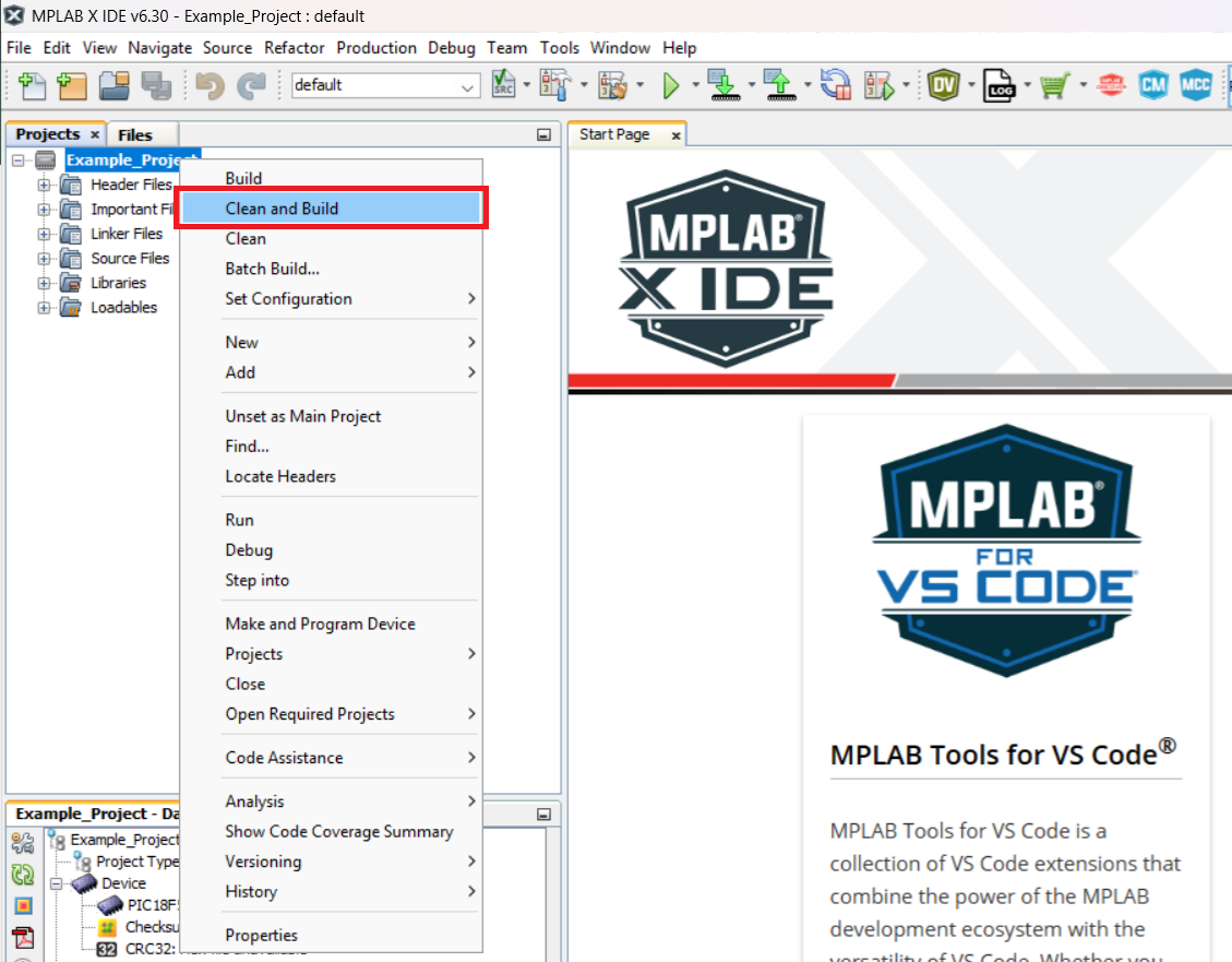
-
Select PICxxxxx Curiosity Nano in the Connected Hardware Tool section of the project settings:
Right click the project and click Properties.
Click the arrow under the Connected Hardware Tool.
Select PICxxxxx Curiosity Nano (click the SN), click Apply and then click OK:
-
Program the project to the board.
Right click the project and click Make and Program Device or directly press the specific button.


